KiCad PCB Design Checklist: 15 Checks Before You Send Gerbers to the Fab
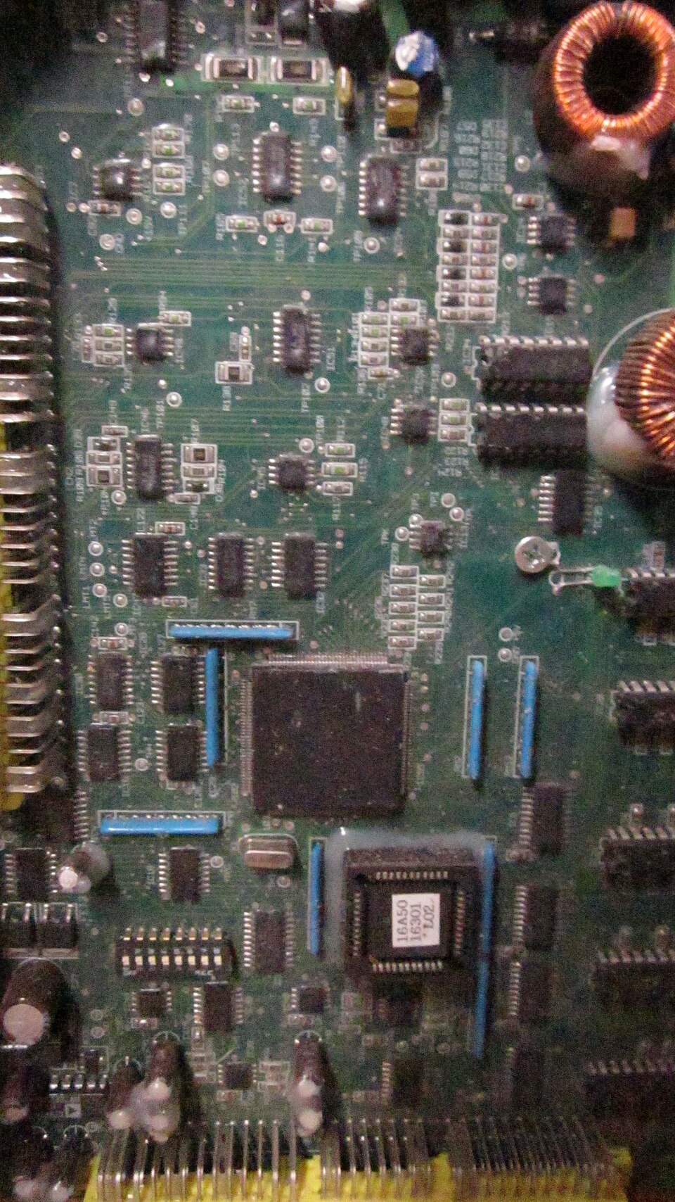
A PCB mistake costs you a week and a new order. This is the checklist we use at ElectroPhobia workshops before ordering a board or etching one in-house: schematic, footprints, layout, design rules and Gerber export in KiCad.
A PCB mistake doesn't show up until the boards arrive, and by then the fix costs a new order and another week or two of shipping. At our KiCad workshops, including the four-day Vector 3.0 pre-event where participants designed, etched and soldered a 555-timer board, we ran the same list of checks before anything went to fabrication.
Here it is, in the order you'd work through a design in KiCad. The examples use KiCad's current releases (version 10 at the time of writing), but the checks apply to any version and any EDA tool.
Schematic
1. Run the Electrical Rules Check (ERC) and read every warning. ERC catches unconnected pins, outputs driving outputs, and power pins with nothing driving them. Don't just dismiss the "power input not driven" error. Add a PWR_FLAG to nets fed from a connector or battery, so KiCad knows they're supplied.
2. Check every net label for typos. In KiCad, VCC and Vcc are different nets. So are SDA and SDA1. A typo silently splits one net into two, and the board ships with an open circuit.
3. Add decoupling capacitors to every IC. One 100 nF ceramic capacitor per power pin is the usual starting point, plus a bulk capacitor (10 µF or more) where power enters the board. They're easy to forget on a schematic because the circuit "works" in simulation without them.
Footprints
4. Verify each footprint against the part you will actually buy. This is the most expensive mistake on the list. A symbol says "transistor", but transistors come in many packages, and the same package can have different pinouts. A TO-92 might be EBC or CBE depending on the part. Open the datasheet's package drawing and compare pin 1 and the pad positions with the footprint.
5. Check the pin-number mapping, not just the package. Symbol pin 1 must be footprint pad 1, and both must match the datasheet. SOT-23 transistors and voltage regulators are frequent offenders: two regulators in the same SOT-223 package can have different input/output/ground pin orders.
6. Print the layout 1:1 and place the real parts on it. It sounds old-fashioned, but it catches wrong hole sizes, connectors that don't fit, and modules (an ESP32 DevKit, a TP4056 board) whose header spacing is different from what you assumed.
Layout
7. Draw a closed board outline on Edge.Cuts. The outline must be a single closed shape, with no gaps or overlapping segments. Fabs reject open outlines, or guess at what you meant. This is how our heart-shaped PCB got its shape: the curve is just an Edge.Cuts outline.
8. Place parts before routing, starting with what's fixed. Connectors, mounting holes, buttons and anything that must line up with an enclosure goes first. Then put decoupling capacitors as close as possible to the pins they serve, with short connections to the ground.
9. Size traces for their current. Signal traces can be thin, but power traces carry real current. IPC-2221 relates trace width, copper thickness and temperature rise. Use a trace-width calculator (KiCad's built-in Calculator Tools has one) rather than guessing. As a rough starting point on standard 1 oz copper, use noticeably wider traces for motor and battery paths than for signals.
10. Use a ground pour, and check it for islands. A filled ground zone on the bottom layer (or both layers) gives a low-impedance return path and makes routing easier. After filling (press B in the PCB editor), look for isolated copper islands that aren't connected to anything, and stitch the layers together with vias.
11. Label everything on the silkscreen. Component references, connector pinouts (VCC GND SDA SCL), polarity marks for diodes, LEDs and electrolytic capacitors, and pin 1 markers on ICs. When you're soldering at 1 am, the silkscreen is your only documentation. Add the board name and a version number too: "v1.1" saves confusion later.
Design rules
12. Set your fab's design rules before routing, and run DRC at the end. Every manufacturer publishes minimum trace width, spacing, drill size and annular ring. In Board Setup → Design Rules, enter them (or slightly more conservative values) before you route, so the router keeps you within limits. Then run the Design Rules Checker and fix everything it reports, including unconnected items.
For in-house etching, use much more relaxed rules. Home-made boards made with UV exposure and HCl + H₂O₂ etching, like at our in-house fabrication workshop, don't reproduce fine features reliably. Wider traces, larger clearances and bigger pads make the difference between a board that works first time and one that needs repair with jumper wires. Single-sided designs are also far easier to etch at home.
Gerbers and drill files
13. Export the right layers. For a typical two-layer board: F.Cu, B.Cu, F.Mask, B.Mask, F.Silkscreen, B.Silkscreen, Edge.Cuts, and paste layers if you're ordering a stencil. Then generate the drill files (Excellon) from the same Fabrication Outputs menu. Many fabs publish a KiCad-specific export guide, so follow theirs.
14. Open the Gerbers in a viewer before uploading. KiCad ships with GerbView, and most fabs show a preview after upload. Check that the outline is there, the drill holes line up with pads, the silkscreen isn't printed over pads, and nothing is mirrored. What you see in the Gerber viewer is what gets made, not what you see in the PCB editor.
15. Zip, upload, and read the fab's preview carefully. Confirm the board dimensions it detects match your design, and pick sensible options: 1.6 mm FR-4, HASL finish and standard colours are the cheapest and fastest for prototypes.
After the boards arrive
Before soldering anything, do a continuity check between VCC and GND on a bare board. A beep means a short in the copper itself. Then solder the power section first, check the voltages, and only then add the chips. Our multimeter guide covers the continuity test.
Learn KiCad from scratch
The free KiCad PCB design track in the ElectroLab course goes from schematic capture to a board you can order, step by step.
References
- KiCad, Official Documentation (Schematic Editor, PCB Editor, Gerber export): docs.kicad.org
- KiCad, Downloads (current stable release): kicad.org/download
- Saturn PCB Toolkit (IPC-2221 trace width and via calculators): saturnpcb.com
- NextPCB, PCB Capabilities (typical design rules for prototype boards): nextpcb.com